Optical microscope JEM-F200TEMSTEMlaboratory

Add to favorites
Compare this product
Characteristics
- Type
- optical, TEM, STEM
- Applications
- laboratory, multipurpose
- Observation technique
- dark field
- Configuration
- floor-standing
- Other characteristics
- ultra-high resolution
- Resolution
0.14 nm, 0.16 nm, 0.19 nm, 0.23 nm
Description
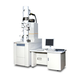
The JEM-F200 is a field emission transmission electron microscope, which features higher spatial resolution and analytical performance coupled with intuitive user interface for multi-purpose operation.
Features
High-resolution TEM/STEM observations from high to low acceleration voltages
The JEM-F200 offers a cold field-emission electron gun, which guarantees high stability, high brightness, and high energy resolution (<0.33 eV).
This electron gun effectively achieves higher-resolution imaging by minimizing chromatic aberrations originating from the energy spread of the electron source.
Furthermore, by incorporating JEOL's 10+ years of expertise into the design, we have significantly improved both mechanical and electrical stability.
High-throughput and high-accuracy EDS analysis
The JEM-F200 can be equipped with two large-area Silicon Drift Detectors (SDD) simultaneously, providing high-sensitivity analysis.
The large area and high sensitivity enables efficient EDS analysis at a fraction of the time with reduced damage.
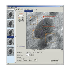
Additionally, utilizing high-speed, lossless drift correction via live STEM images during EDS mapping enables efficient measurements while reducing sample damage from the electron beam.
EELS analysis with high energy resolution
The CFEG of the JEM-F200 can obtain analysis of chemical bonding states and electronic structure at high energy resolution, surpassing the capabilities of a Schottky field emission electron gun.
This is made possible by incorporating a cold field-emission electron gun that guarantees high energy resolution (<0.33 eV) with EELS (option).
Easy operation with minimal stress even for beginners
VIDEO
Catalogs
No catalogs are available for this product.
See all of Jeol‘s catalogsRelated Searches
- Analysis medical software
- Microscopy
- Compound microscope
- Laboratory microscope
- Tabletop microscope
- Microscope with LED light
- Viewer software
- Clinical chemistry analyzer
- Laboratory software
- Windows medical software
- Automatic clinical chemistry analyzer
- Benchtop clinical chemistry analyzer
- Reporting software
- Acquisition software
- Treatment software
- Biological microscope
- Measurement software
- Blood clinical chemistry analyzer
- Binocular microscope
- Research microscope
*Prices are pre-tax. They exclude delivery charges and customs duties and do not include additional charges for installation or activation options. Prices are indicative only and may vary by country, with changes to the cost of raw materials and exchange rates.


